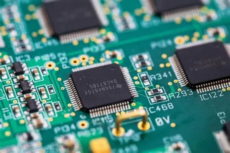
The semiconductor industry is undergoing a massive transformation, and the United States is at the center of this shift. Fueled by the CHIPS Act and the urgent need to secure domestic chip production, several leading global and U.S. companies are investing billions in new fabrication plants — or “fabs.” These facilities, some among the largest industrial projects in recent U.S. history, are reshaping local economies, driving construction demand, and creating high-tech infrastructure at an unprecedented scale.
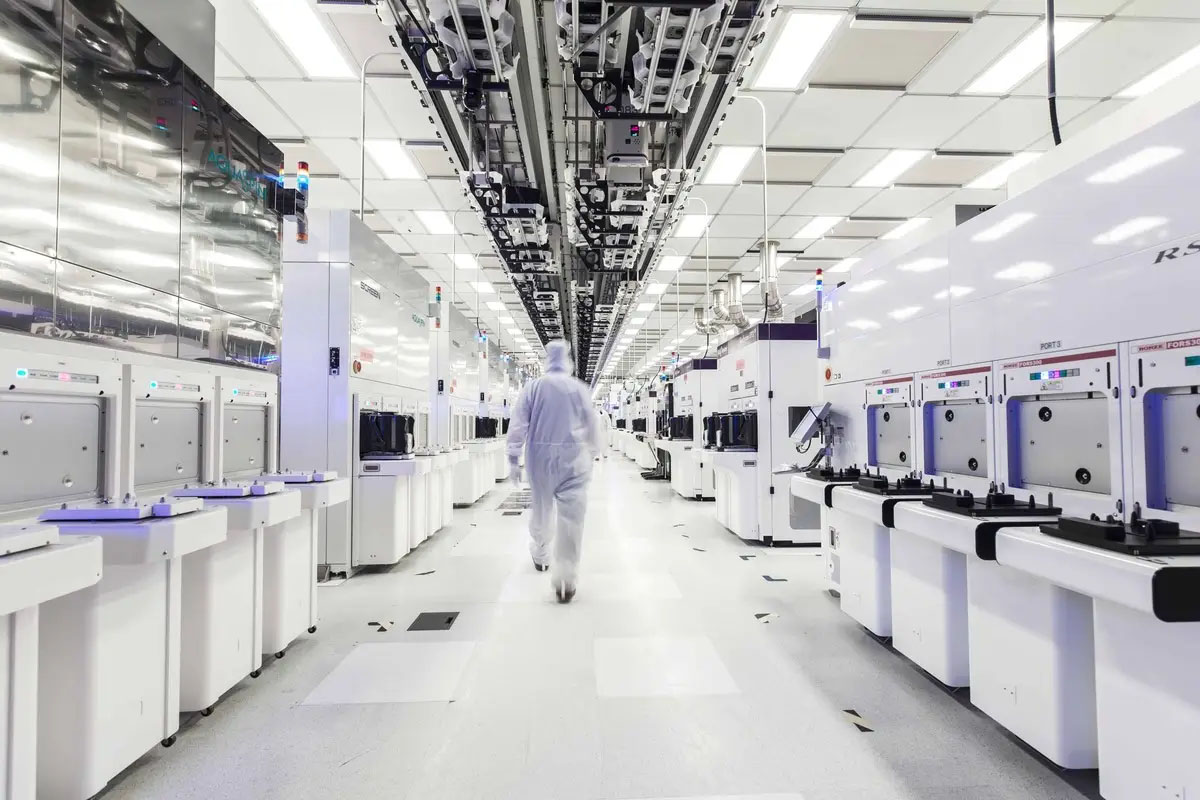
For construction professionals, these projects are more than just factories; they are massive, high-tech building endeavors requiring advanced planning, precision engineering, and specialized construction techniques. Let’s take a closer look at some of the key semiconductor plants currently under development.
SK Hynix – $4.09B West Lafayette, Indiana
SK Hynix is set to launch a state-of-the-art memory chip packaging and research facility in West Lafayette, Indiana, with a total investment of $4.09 billion. The U.S. government is providing $450 million in grants and $500 million in loans under the CHIPS and Science Act, along with a 25 % tax incentive on capital investments. The 430,000-square-foot facility on a 90-acre site will focus on next-generation high-bandwidth memory (HBM) chips for AI applications.
The project, expected to reach full operational capacity by late 2028, will create a wide range of jobs in engineering, technical support, administration, and maintenance. SK Hynix will collaborate with Purdue University and Ivy Tech Community College for R&D and workforce training programs. The facility strengthens U.S. leadership in AI memory chip production and advanced semiconductor research, complementing broader federal efforts to boost domestic chip manufacturing and secure critical supply chains.
Advancement on the project is picking up pace as SK hynix is set to commence full-scale foundation work on the advanced HBM packaging plant in Indiana starting end of February. The company plans to accelerate the plant’s construction to respond to mid and long term demands for High Bandwidth Memory (HBM). The move comes at a time when competition in A.I chips is shifting to advanced packaging competition. Advanced packaging, which belongs to the back-end process of HBM production, is a core technology that determines HBM yield and performance.
According to industry sources earlier this week, the client company will install fencing the advanced semiconductor chip manufacturing plant construction site in West Lafayette starting from Feb. 23. Afterwards, it will begin preliminary construction work.
Wolfspeed – $5B Siler City, North Carolina
Wolfspeed is close to completing its $5 billion semiconductor factory in Siler City, Chatham County, North Carolina. The 2.2 million-square-foot facility, with room for an additional 2 million square feet, will manufacture advanced 200 mm silicon carbide crystals—key components for electric vehicle technology. Company officials expect to take full control of the plant by March 2025, with production slated for June 2025.
The project received over $700 million in state and local incentives, with most contingent on meeting hiring benchmarks. At full operation, the factory will employ around 1,800 workers, while peak construction involved 3,800 personnel. Some crystal production testing is already underway. Wolfspeed is also pursuing federal support through the CHIPS Act to strengthen U.S. semiconductor competitiveness.
This factory is part of North Carolina’s recent industrial boom, alongside Toyota’s Randolph County facility and Fujifilm Diosynth’s expansion, reinforcing the state’s role in domestic semiconductor manufacturing and advanced EV technology supply chains.
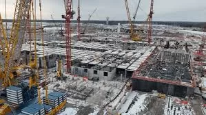
Micron $100B Clay, Megafab New York
Micron’s $100 billion semiconductor megafab in Clay, New York, has been significantly delayed. Fab 1 construction will now break ground this January 2026, with operations starting around Q3 2030, two years later than planned. Fab 2 will begin construction in late 2030, with operations expected by 2033. The full four-fab buildout is projected to complete by 2041, with full-scale production by 2045. About $1.2 billion in CHIPS Act funding is being reallocated to boost Micron’s Idaho facility.
New York regulators approved a critical 345 kV, two-mile underground transmission line linking the Clay substation to the plant, resolving a key energy infrastructure hurdle. The megafab is expected to create over 50,000 jobs over 20 years, including 9,000 direct Micron roles, and could supply up to 25 % of U.S.-made semiconductors by 2030. The project underscores the importance of energy capacity, environmental planning, and grid upgrades for large-scale high-tech investments in the U.S.
Intel – $20B New Albany, Ohio
Intel Corporation’s $20 billion Ohio One chip plant in New Albany, Licking County, is the largest investment in Ohio’s history. Announced in January 2022, the project involves constructing two advanced semiconductor factories, with initial site preparation beginning in July 2022 and a groundbreaking ceremony held in September 2022, attended by President Joe Biden.
The first year focused on leveling land, excavating utility trenches, and pouring 2.5 million square feet of concrete foundations. The project is expected to create around 3,000 direct jobs and 7,000 construction positions, with additional employment through suppliers and local services.
Ohio One will produce advanced chips for Intel and other manufacturers, supporting applications from data centers to smart devices. While originally targeted for 2025, Intel has since adjusted the construction timeline, with the first plant now expected in 2030. Local infrastructure and education initiatives, including new roads and semiconductor-focused programs, are underway to support workforce and community needs.
Amkor – $7B Peoria, Arizona
Amkor Technology has broken ground on its expanded semiconductor advanced packaging and test campus in Peoria, Arizona, increasing its investment from $2 billion to $7 billion across two phases. The project will be Amkor’s first high-volume U.S. advanced packaging facility, covering over 750,000 square feet of cleanroom space, including a second greenfield facility. Construction of the first facility is scheduled for mid-2027, with production expected in early 2028, serving clients such as Apple and NVIDIA.
The campus will create up to 3,000 jobs and provide end-to-end packaging and testing capabilities, complementing TSMC’s wafer fabrication operations in Arizona. Supported by federal and state programs including the CHIPS Act, the expansion integrates smart factory technologies to meet rising demand in AI, high-performance computing, mobile, and automotive sectors. The project underscores the growing trend of U.S. semiconductor investment, strengthening domestic supply chains and advancing the country’s leadership in advanced chip technologies.
Micron – $30B Boise, Idaho
Micron Technology is set to build a second leading-edge memory fab in Boise, Idaho, as part of its broader $200 billion U.S. investment program to boost domestic semiconductor production and R&D. The new $30 billion investment will also support the expansion of Micron’s Manassas, Virginia, facility and in-house High Bandwidth Memory (HBM) packaging capabilities, critical for AI and high-performance computing.
Co-located with Micron’s existing R&D hub and first Boise fab, the second plant will accelerate product development and reduce time-to-market, with production expected before Micron’s first New York fab comes online. The Idaho expansion is projected to create over 17,000 jobs, while the overall U.S. investment could generate around 90,000 direct and indirect roles across construction, engineering, and manufacturing. Workforce development programs, including apprenticeships and university partnerships, support this growth. Micron’s initiative strengthens the domestic memory supply chain, advancing America’s technological leadership in AI and high-performance computing, alongside broader U.S. semiconductor developments like Samsung’s Texas plant.
Bosch – Upgrade $1.9B Roseville, California
Bosch is upgrading its semiconductor plant in Roseville, California, with a total investment of $1.9 billion, including up to $225 million in CHIPS Act funding. Rather than building a new facility, Bosch is renovating its existing plant to produce advanced 200mm silicon carbide chips for electric vehicles, charging systems, and power electronics, with production expected in 2026.
The company retained nearly all 250 employees from TSI Semiconductors and provided extensive training through its global manufacturing network. Construction is carried out under a project labor agreement with the Sacramento-Sierra Building and Construction Trades Council.
The project aligns with the U.S. strategy to strengthen domestic semiconductor manufacturing and advance electrification, supporting local high-tech job retention and regional infrastructure development. Bosch’s investment reflects confidence in the skilled Roseville workforce and the growing demand for EV-related semiconductor technologies. This initiative is part of a broader trend, highlighted by Samsung’s resumed $4 billion Texas plant construction, boosting America’s semiconductor ecosystem.
Samsung Electronics – Cost $4B Taylor, Texas
Samsung Electronics has restarted construction on its massive semiconductor facility in Taylor, Texas, following a 2024 pause due to global chip demand slowdown. The project is backed by a fresh $4 billion investment, including $2.87 billion for critical manufacturing equipment, and will create thousands of high-tech jobs. Hiring for engineers will occur in two phases starting September and November 2025, overseen by a dedicated project head.
The restart is fueled by a new contract with Tesla for next-generation 2nm chips, ensuring demand for advanced semiconductors that will power future electric vehicles and AI systems. The plant will use Samsung’s SF2P process, strengthening the U.S. semiconductor supply chain and boosting domestic production. Originally planned as an $18 billion 5nm EUV facility in Austin, the project reflects Samsung’s commitment to U.S. growth and is expected to deliver long-term economic benefits while advancing technology innovation.
Albany NanoTech Complex – Cost $10B Upstate New York
A $10 billion public–private expansion led by NY Creates is positioning the Albany NanoTech Complex to make Upstate New York a global leader in semiconductor research, development, and emerging manufacturing. The initiative combines major facility growth, advanced chipmaking equipment, workforce development, and partnerships with universities and industry to strengthen U.S. semiconductor innovation and supply chains. As part of this effort, the campus is being upgraded to host leading-edge tools that only a few sites worldwide can support.
A key milestone in the expansion is the topping out of NanoFab Reflection, a $1 billion, 310,000-square-foot research building that will house the nation’s first publicly owned High NA EUV lithography system when it arrives in 2026. This cutting-edge technology will enable the development of smaller, faster, and more energy-efficient chips. Supported by partners such as IBM, Micron, Applied Materials, and Tokyo Electron, the project is expected to generate thousands of high-tech jobs, attract billions in private investment, and solidify New York’s leadership in next-generation chip innovation.
Why These Projects Matter for Construction
Semiconductor plants are some of the most complex industrial projects in the world. They require:
-
Specialized construction techniques: From cleanroom floors to vibration-free foundations.
-
High-precision utilities: High-voltage electricity, ultra-pure water, and chemical pipelines.
-
Long-term planning: Multi-year construction timelines with phased expansion.
-
Workforce coordination: Thousands of engineers, technicians, and construction workers.
For contractors, engineers, and suppliers, these projects present significant opportunities for collaboration and innovation.
Conclusion
The U.S. semiconductor build-out is more than a technology story — it is a construction and engineering challenge of historic scale. From Arizona to Ohio, Idaho, New York, Texas, and Utah, these fabs are reshaping local economies, creating thousands of construction jobs, and setting a benchmark for high-tech industrial development. For the construction industry, they represent a new era of precision, scale, and opportunity — a testament to how industrial construction and technology innovation intersect.
As these projects continue to rise from the ground, they offer a clear signal: the future of construction is not just about buildings; it is about building the backbone of next-generation technology.
Leave a Reply