
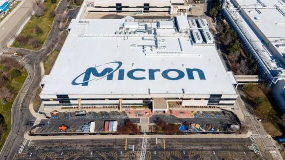
An engineering, procurement and construction (EPC) contract has been awarded to Bechtel for the first phase of Micron Technology’s semiconductor manufacturing complex in Clay, New York, marking a major step forward in the development of what is planned to become the largest semiconductor manufacturing facility in the United States.
Under the agreement, Bechtel will begin mobilizing immediately at the White Pine Commerce Park site in Onondaga County as Micron advances construction of the project. The announcement comes several months after Micron broke ground on its first New York fabrication plant in January 2026.
The manufacturing complex forms part of Micron’s long-term investment strategy to expand advanced memory chip production in the United States. Once fully developed, the facility is expected to support growing demand for memory technologies used in artificial intelligence, data centers and other advanced computing applications.
New jobs
According to Micron, the project is expected to create approximately 50,000 jobs across New York over the coming decades, including more than 4,500 construction positions. During peak construction, thousands of skilled trade workers, contractors, suppliers and construction professionals are expected to be involved in the development.
Economic impact
Micron estimates the project could contribute approximately US$16.7 billion annually to New York’s economy and generate around US$5.4 billion in personal income each year over a 30-year period.
As EPC contractor, Bechtel will oversee engineering, procurement and construction activities for the first phase of the project. The company said it plans to use an integrated delivery approach incorporating engineering services, procurement management, modular construction strategies and digital construction technologies.
Semiconductor fabrication facilities are among the most complex industrial developments globally, requiring highly controlled manufacturing environments, advanced electrical systems, cleanroom infrastructure and precision construction techniques.
The project is also expected to contribute to broader efforts aimed at expanding domestic semiconductor manufacturing capacity and strengthening the resilience of the U.S. technology supply chain.
The project is among several large-scale semiconductor manufacturing investments underway in the United States. It joins projects such as Intel’s Ohio One campus in New Albany, Ohio, where the chipmaker is investing more than $20 billion in two leading-edge fabrication plants aimed at expanding domestic semiconductor production capacity.
Micron New York Semiconductor Manufacturing Complex: Factsheet
Project overview
Project: Micron New York Megafab (Central New York Semiconductor Manufacturing Facility)
Location: 5171 Route 31, Clay, Onondaga County, New York (White Pine Commerce Park)
Proximity: 10 minutes outside Syracuse, upstate New York
Project Type: Leading-edge DRAM semiconductor manufacturing facility
Investment: Up to $100 billion over 20+ years
Classification: Largest private investment in New York state history; largest semiconductor investment in NY
Facility specifications
Number of Fabs: Up to 4 high-volume manufacturing (HVM) fabs
Chip Type: Leading-edge DRAM using EUV lithography
Cleanroom per Fab: 600,000 sq ft
Total Cleanroom: 2.4 million sq ft (equivalent to 40 U.S. football fields)
Cleanroom Record: Largest cleanroom ever announced in the United States
Site Size: 1,400-acre White Pine Commerce Park
Job creation and economic impact
Total New York Jobs: Nearly 50,000 over 20+ years
Direct Micron Jobs: 9,000 high-paying positions
Community Jobs: 40,000+ ancillary roles (suppliers, contractors, supporting industries)
Construction Jobs: 4,500+ (Bechtel partnership, June 2026)
Timeline
Project Announced: 2022
Site Preparation Begins: 2023
CHIPS Act Funding Awarded: 2024 ($6.165 billion)
Gilbane Preconstruction Contract: August 2025
Timeline Delay Announced: November 13, 2025
Official Groundbreaking: January 16, 2026
Air Title V Permit Issued: March 2026
Workforce Partnership Launched: April 29, 2026
Bechtel EPC Partner Selected: June 10, 2026 (Latest)
First Fab Construction (Q2): 2026
First Fab Operational: Q3 2030
Second Fab: 2033
Third Fab: 2038
Fourth Fab: 2041
Full Production Capacity: 2045
Funding and public support
Total Public Funding: Approximately $25 billion
Federal CHIPS Act: $6.165 billion
New York State Incentives: $5.5 billion
Additional State Support: Approximately $1.5 billion
Green CHIPS Community Fund: $250 million (Micron contribution)
Additional Community Investment: $250 million ($100 million state, $150 million partners)
Infrastructure and resources
Daily Water Usage: 48 million gallons from Lake Ontario
Water Treatment: New wastewater plant planned by Onondaga County
Electricity Target: 100% renewable
Wetlands: Project fills over 200 acres (environmental concern)
Technology
Lithography: Extreme Ultraviolet (EUV)
Production: Multiple generations of DRAM
U.S. DRAM Target: Increase from less than 2% to 40% of Micron’s global output in next decade
Regional Impact: By 2030s, one in four U.S.-made chips within 350 miles of upstate New York
Current status (June 2026)
Phase: Active construction (post-groundbreaking)
Construction Partner: Bechtel (selected today, June 10, 2026)
Activity: Bechtel mobilizing immediately; scaling up quickly
Next Milestone: First fab construction beginning Q2 2026
Status: On track with updated timeline
Key partners and organizations
Micron Technology: Project owner (Nasdaq: MU)
Bechtel: EPC partner (June 2026)
Gilbane: Preconstruction contractor (August 2025)
NY Creates: Workforce development partnership
Empire State Development: esd.ny.gov/micron
NYSDEC: Permitting agency
Leave a Reply