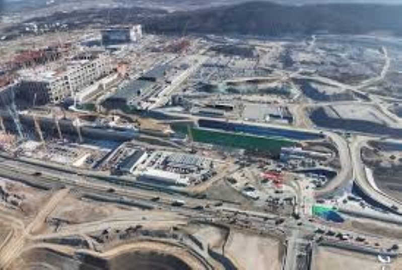
The South Korea semiconductor mega-cluster led by Samsung Electronics and SK Hynix is accelerating into a new phase in 2026, as the global artificial intelligence (AI) boom reshapes chip investment priorities and pushes memory demand to record levels.
Yongin-Pyeongtaek corridor, the world’s largest semiconductor manufacturing hub, saw new investment momentum early 2026 after SK Hynix unveiled plans in April and February to pour more than US$27bn into new advanced packaging and AI-memory production facilities in Yongin through 2030. This is while speeding up factory commissioning schedules to tackle tightening global supply constraints. The changes in schedule also includes plans by Samsung to advance start of chip fab plant at Yongin to 2029, up to two years earlier than previously planned.
At the same time, soaring valuations and profits are being witnessed at both Samsung and SK Hynix, driven largely by high-bandwidth memory (HBM) demand from AI data centers. This reinforces the importance of the mega-cluster in South Korea. Seoul is also intensifying efforts to secure supply-chain resilience, expand its domestic chip infrastructure and cement South Korea’s dominance in next-generation semiconductors. Effectively, more semiconductor investments are being driven in to the East Asia region, with some of the latest including Samsung’s US1.5$ bn chip testing plant in northern Vietnam.
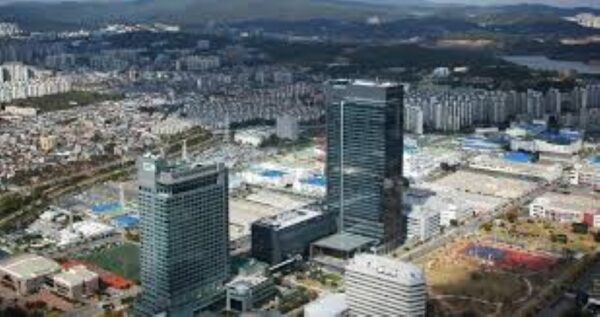
South Korea’s US$471 Billion Semiconductor Mega-Cluster
Reported March 5, 2026 – The South Korea semiconductor mega-cluster is a US$471 billion (622 trillion won) chip-making hub being developed across the Pyeongtaek-to-Yongin corridor in Gyeonggi Province, South Korea, anchored by Samsung Electronics and SK Hynix. It aims to become the world’s largest chip production region by 2030.
The cluster will add 13 new fabrication plants and three research facilities to the existing 21 fab centers. It also targets a production capacity of 7.7 million wafers per month and an estimated 3.46 million jobs. SK Hynix broke ground at the Yongin site in March 2025, with the first clean-room facility targeted for completion by 2027.
Total projected investment in the Yongin cluster alone has since risen to approximately 600 trillion won. This is driven by surging AI and HBM demand, with Samsung also committing 450 trillion won domestically over the next five years. The scale of this industrial build-out is also reshaping Gyeonggi Province more broadly. This is so as major public infrastructure follow in its wake – including the recently signed $427 million Siheung Baegot Seoul National University Hospital, an 800-bed facility designated as an AI Advanced Medical Demonstration Hub. It is designed to anchor a new bio-industry and healthcare ecosystem in the region.
Project Overview
Type: National semiconductor mega-cluster (fabs, R&D centers, and supporting industry)
Location: Pyeongtaek to Yongin, Gyeonggi Province in South Korea
Total planned investment: 622 trillion won (US$471 billion) through 2047
New facilities: 13 chip plants and 3 research facilities (on top of 21 existing fabs)
Target production capacity: 7.7 million wafers/month by 2030
Cluster footprint: 2,102 square meters
Power requirement: 3GW initially, scaling to 10GW
Job creation: 70,000 direct jobs; 3.46 million total estimated
Logic chip market share goal: 10% by 2030 (up from 3%)
SK Hynix Yongin groundbreaking: March 2025; first fab clean-room targets 2027 construction start. Samsung Pyeongtaek Line 5 (P5) construction resumed late 2025 with commercial operations targeted for 2028.
Power supply: Connected to hydroelectric and national grid. Supporting infrastructure managed by Ministry of Trade, Industry and Energy (MOTIE)
Investment and Infrastructure Breakdown
Samsung investment commitment: Initially 500 trillion won (US$370B) by 2047. Revised to 450 trillion won domestically over next 5 years
SK Hynix investment commitment: Originally 122 trillion won. Currently projected to reach 600 trillion won for Yongin cluster alone
Samsung fab breakdown: 6 new fabs at Yongin (360T won), 3 fabs at Pyeongtaek (120T won), 3 R&D fabs at Giheung (20T won)
SK Hynix fab plan: 4 fabs at Yongin cluster, focused on HBM4, HBM4E, and 321-layer NAND
Supporting infrastructure: MOTIE power supply task force; BC Hydro-equivalent grid expansion underway
Chip focus: High Bandwidth Memory (HBM), DRAM, 2nm and below logic chips, system semiconductors
Project Developers and Stakeholders
Government lead: South Korean Ministry of Trade, Industry and Energy (MOTIE)
Minister: Ahn Duk-geun, MOTIE
Lead companies: Samsung Electronics, SK Hynix
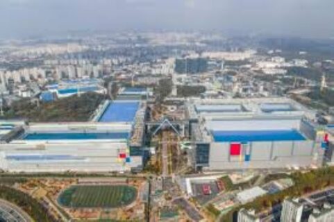
US$471 bn Chip-Making Hub Planned in South Korea, Samsung Electronics and SK Hynix Feature in Plans
Reported January 16, 2024 – South Korea plans to build US$471 billion chip-making hub in collaboration with Samsung and SK Hynix.
By 2030, the Pyeongtaek to Yongin region in South Korea is anticipated to become the leading chip-making hub globally. It aims for a 7.7 million wafer production capacity cap monthly. This will make is the largest chip hub in the world.
Investments totalling 622 trillion won (US$471 billion) from semiconductor companies will ensure the security of domestic chip supply. This investment has 2047 in sights. The investment will also secure and fortify the nations chip supply. This will allow for participation in the competition for technological self-sufficiency.
Number of Chip Plants Planned in the South Korea Semiconductor Mega-Cluster
South Korea has plans to invest in the building of 13 chip plants and three research facilities in addition, to the existing 21 fabs. This development will cover a region, from Pyeongtaek to Yongin making it the largest chip production area globally. It is estimated that by 2030 this expanded setup will have the capacity to manufacture 7.7 million wafers every month.
The planned investment for building the chip-making hub by South Korea has significantly increased since Seoul initially announced the plans of Samsung and Hynix in 2023. The Korean government, known for collaborating with private companies, on national priorities has been actively increasing its support, for the domestic chip industry, which contributes around 16 percent to the country’s total exports.
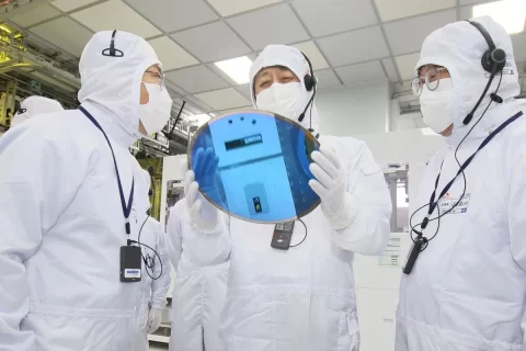
The government of South Korea is also dedicated to safeguarding an aspect of its economy amidst increasing competition. In response, to the growing investments in chip-making sectors, by Japan and Taiwan the Korean government is taking measures to provide tax incentives to domestic chip companies.
Read also: Samsung Electronics expands its foundry capacity with a new production line in Pyeongtaek, Korea
Samsung and SK Hynix’s Share in the Growing South Korea Chip Market
As part of their long term strategy, Samsung and Hynix have plans to build more chip manufacturing facilities across Southeast Asia. Samsung’s emphasis is on the foundry sector. This is part of a 500 trillion won investment plans by 2047. Meanwhile SK Hynix, a competitor, is targeting an investment of 122 trillion won in memory technology in Yongin over the same time-frame.
Other Investments by Samsung and SK Hynix
Besides the plan by South Korea to build a chip-making hub, Samsung and SK Hynix also have intentions to make additional investments.
Samsung plans to allocate a budget of KRW480 trillion ($363 billion) towards establishing manufacturing facilities and production lines. On the hand SK Hynix has also earmarked KRW122 trillion ($92 billion) for its chip business. This will be used for the construction of a memory chip plant.
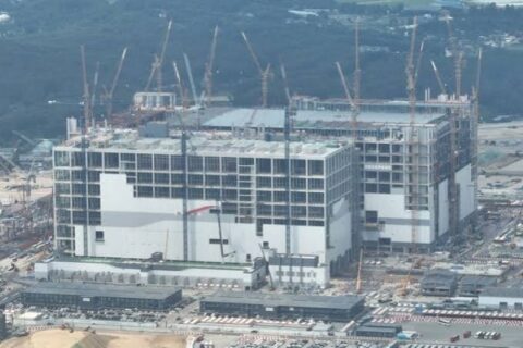
South Korea has also announced plans to build a smaller hub for chip design and materials companies in the region. The main goal is to enhance the country’s self-reliance in semiconductors. Also within sights is the expansion of its share in chip production. The goal is a 10% market share by 2030, up from the 3 percent.
The chip-making hub is projected to need a power capacity of 3 gigawatts with growth, to 10GW. To give you a sense of scale the largest nuclear power plant currently operating in South Korea generates over 7.6 GW of electricity.
Outlook on the South Korea Semiconductor Mega-Cluster
As South Korea plans the development of the mega chip-making and fab hub, employment opportunities will also be on the rise. 70,000 skilled professionals along with an additional 40,000 positions at companies that provide parts and materials are expected. Additionally, considering the effect on job creation from the hub, South Korea estimates that this project will potentially generate employment for around 3.46 million individuals during its lifetime.
Read also: New York teams up with IBM, Micron for $10B semiconductor facility at Albany University
Read also: Amkor plans to build $2B semiconductor packaging and testing facility in Peoria, AZ