Taiwanese chipmaker GlobalWafers is preparing for the second phase of expansion at its chip facility in Sherman, Texas. The move on expansion has been sparked by the recent surge of customer demand as noted by chairperson Doris Hsu. The decision resulted from conversations with multiple customers who told the company they would like capacity at the site to increase. “Regarding additional investment, we have started to be asked by customers,” said Hsu. ” We think phase one may not be enough, because phase one does not serve just one customer but multiple customers.”
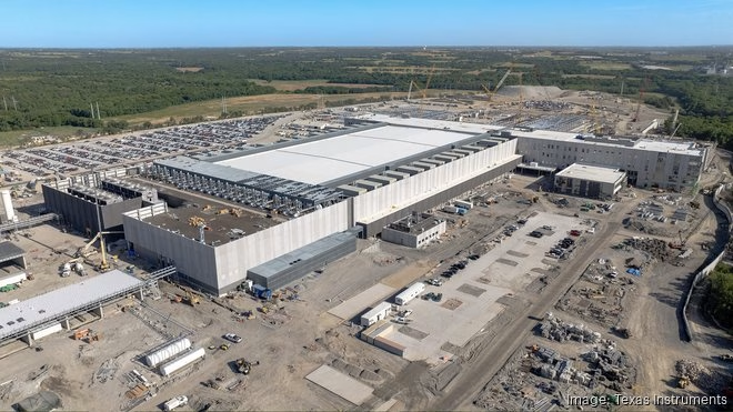
Furthermore, he noted that each of these customers have mentioned that they would like capacity to increase. GlobalWafers opened its $3.5 billion chip fab in Sherman in May 2025. At the time, the chipmaker also announced plans to invest an additional $4 billion in the U.S. The 142-acre campus in Texas can accommodate up to six phases. Moreover, while no timeline has been outlined, the company said plans to add two additional phases to the fab were already under way. Alongside the GlobalWafers chip facility, Intel’s Ohio One chip plant is also taking shape. The move shows the significance of chip factories across the U.S.
Scope of Implementation on the GlobalWafers Chip Facility in Texas
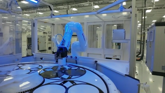
The construction of the GlobalWafers chip facility in Texas has already completed the first phase. Moreover, they noted that Phase II is still in planning. Hsu had previously said that for the company to move forward with further capacity increases, Phase I and II “must be profitable.” In total, GlobalWafers has facilities in nine countries, including a second fab in St. Peter’s, Missouri. At both its US sites, the company produces 300-mm wafers and silicon-on-insulator wafers. The company is also planning to convert its existing silicon epitaxy wafer manufacturing facility in Sherman. Plans are to convert it to a silicon carbide (SiC) epitaxy wafer manufacturing site, producing 150mm and 200mm SiC epitaxy wafers.
Project Factsheet
Project Location
• Sherman, Texas, United States
• 142-acre campus with capacity for up to six development phases
Current Status
• Phase I completed and operational (opened May 2025)
• Phase II in planning, with additional phases under evaluation
• No fixed timeline announced for subsequent phases
Investment Profile
• Initial Investment: $3.5 billion
• Additional U.S. Investment Announced: $4 billion
• Expansion decisions linked to profitability of Phases I and II
Production Scope
• Manufacturing of 300mm wafers
• Production of silicon-on-insulator (SOI) wafers
• Serves multiple customers rather than a single anchor client
Technology Expansion
• Planned conversion of existing Sherman facility
• Shift toward silicon carbide (SiC) epitaxy wafer manufacturing
• Output to include 150mm and 200mm SiC epitaxy wafers
Strategic Context
• Expansion aligns with growing U.S. semiconductor demand
• Strengthens GlobalWafers’ U.S. manufacturing footprint
• Complements existing U.S. fab in St. Peters, Missouri
Global Footprint
• Operations across nine countries
• Texas facility positioned as a long-term, scalable production hub
Leave a Reply