
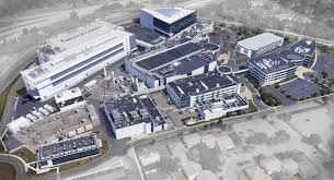
Last month, construction reached a major milestone on NanoFab Reflection, a $1 billion semiconductor research facility being built by NY Creates at the Albany NanoTech Complex. The project has now “topped out,” with the final steel beam placed, marking the 310,000-square-foot structure as complete and moving into interior build-out and equipment preparation. The facility is being built to house the United States’ first publicly owned High NA EUV lithography center, a next-generation toolset used to develop advanced computer chips. The topping-out marks the installation of the building’s final steel beam and confirms the project is progressing on schedule.
NanoFab Reflection will expand the Albany NanoTech Complex—already one of the nation’s leading semiconductor R&D sites—by adding 50,000 square feet of cleanroom space. The facility will host ASML’s High Numerical Aperture Extreme Ultraviolet (High NA EUV) lithography system. The most advanced chip-patterning equipment in development. Researchers and industry partners will begin using the machine when it arrives in 2026 to develop the next generation of smaller, faster, and more energy-efficient chips.
The project is part of a larger $10 billion public–private expansion underway at the Albany NanoTech campus. Once fully operational, the new facility is expected to support hundreds of permanent high-tech jobs. And attract additional semiconductor companies, universities, and workforce programs to the region.
High NA EUV capability marks a major milestone for U.S. chip research and domestic supply-chain development. Only a few locations worldwide are preparing to host the equipment, and Albany’s facility will serve as one of the main testing and development centers for the technology.
The NanoFab Reflection team expects to complete the facility by the end of next year, adding another key asset to New York’s growing semiconductor ecosystem.
Elsewhere in the state, Micron plans to break ground Jan. 16 on a $100 billion semiconductor megafab in Central New York. The facility is expected to become the largest semiconductor manufacturing campus in the United States and will expand domestic memory chip production. Together with NanoFab Reflection, these projects highlight New York’s growing role as a hub for advanced semiconductor research and manufacturing, attracting major technology investment and reinforcing the state’s position in the rapidly evolving global chip industry.

NanoFab Reflection Facility at Albany NanoTech Complex: Factsheet
Overview
NanoFab Reflection is a new state-of-the-art semiconductor research and development facility at the Albany NanoTech Complex of NY Creates in Albany, New York.
Facility Specifications
Size: 310,000 square feet total building area
Cleanroom Space: 50,000 square feet of advanced cleanroom for leading-edge semiconductor R&D
Investment: $1 billion state investment
Status: Structure topped out (final steel beam installed); completion expected by end of 2026
Purpose & Capabilities
The facility will contain the first publicly owned High NA EUV (Extreme Ultraviolet) Lithography Center in North America. Housing the most advanced chip-making research equipment in the world.
Key Equipment:
ASML High NA EUV lithography system, set to arrive in mid-2026
Capability to build next-generation chips that will be more powerful, faster, and energy-efficient.
Significance
Greatest Chip research and development capability in the world
Supports hundreds of new permanent high-tech jobs
Expected to generate $9 billion in private investment
Designed to support demanding, leading-edge semiconductor R&D work
Location
Albany NanoTech Complex, Albany, New York
Leave a Reply