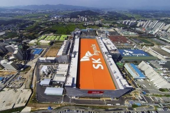
SK hynix is set to commence full-scale foundation work at its $4 billion advanced HBM packaging plant in Indiana starting end of February. The company plans to accelerate the plant’s construction to respond to mid and long term demands for High Bandwidth Memory (HBM). The move comes at a time when competition in A.I chips is shifting to advanced packaging competition. Advanced packaging, which belongs to the back-end process of HBM production, is a core technology that determines HBM yield and performance.
According to industry sources earlier this week, the client company will install fencing the advanced semiconductor chip manufacturing plant construction site in West Lafayette starting from Feb. 23. Afterwards, it will begin preliminary construction work.
Starting from March 2, the company is scheduled to commence preparatory work for main construction. These include ground compaction (grading work) and also civil engineering work at the construction site. The company is hopeful that the expected completion and operation timeline of 2028 will be achieved. The investment amount is $4.09 billion. Moreover, the project is one of the major semiconductor plant projects underway in the United States.
Outlook on the SK hynix Advanced HBM Packaging Plant in Indiana
The advancement works on the advanced HBM packaging plant in Indiana by SK hynix is one that is expected to have no major hiccups. The firm had already had applied for permits for foundation work on various facilities such as office buildings and a Central Utility Building (CUB). The permits also encompassed a semiconductor plant which were approved by the West Lafayette city authorities at the end of last month.
With permits for such foundation work recently being issued, construction work is understood to be gaining momentum. As foundation work is typically followed immediately by the main construction phase, groundbreaking is also anticipated for Q1 this year. “The schedule is proceeding sequentially with the goal of operation in 2028,” an SK hynix official noted. Once complete, SK anticipates to utilize the plant as a next-gen HBM packaging facility.
It also plans to sequentially mass-produce next-generation HBM, starting with the mass production of 6th-generation HBM (HBM4) this year. The company holds a dominant position in the HBM market. Projections also indicate it will supply approximately 70% of HBM4 for NVIDIA’s next-generation AI accelerator ‘Vera Rubin’ this year. SK hynix is expanding its packaging bases not only in the U.S. but also domestically.
Project Factsheet
- Name: SK hynix Advanced HBM Packaging Plant.
- Developer / Owner: SK hynix
- Project Type: Advanced semiconductor packaging facility (HBM back-end process)
- Total Investment: $4.09 billion
- Core Competency: High Bandwidth Memory (HBM) advanced packaging.
Location & Site Details
- City: West Lafayette, Indiana
- State: Indiana, United States
- Site Activity: Fencing of a construction site since February 23.
- Regional Significance: Also increases the U.S. based advanced semiconductor production.
Construction Status & Scope
- Beginning of Foundation Work: February 26.
Preliminary Works Include:
- Site fencing
- Compression of the soil on the ground (grading work).
- Also include civil engineering works
- Main Construction Prep: This is planned to start March 2.
Facilities that were covered by Permits:
- Semiconductor assembly facility.
- Office buildings
- It also entails a Central Utility Building (CUB).
Timeline & Approvals
- Authority Permit: city authorities of West Lafayette.
- Status of Permit: Approved (at the end of the previous month)
- Groundbreaking is also expected in Q1 this year
- Completion& Operation: 2028.
Technology & Strategic Signification.
- Type of Process: Advanced packaging (HBM back-end manufacturing)
- Role in Production: Facilitates HBM yield and also performance.
- Planned Deliverable: NG HBM packing.
Leave a Reply