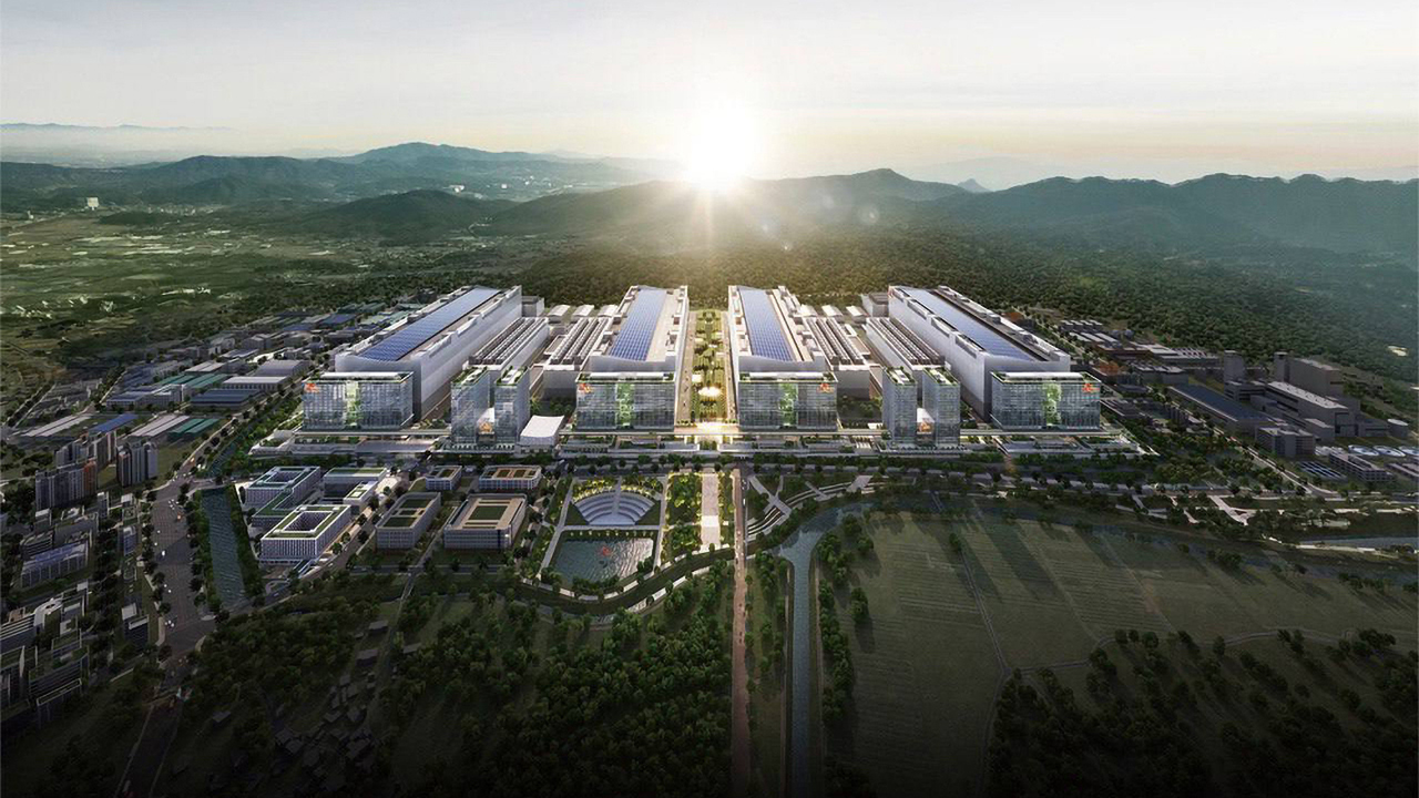
The South Korea semiconductor mega-project is the largest industrial bet the country has ever placed, an 800 trillion won programme worth roughly $518 billion that will plant four new memory chip fabrication plants in the nation’s southwestern region. President Lee Jae Myung unveiled the plan on June 29, 2026 at the Blue House in Seoul, flanked by Samsung Electronics Executive Chairman Lee Jae-yong and SK Group Chairman Chey Tae-won, casting it as a “great leap forward” built on what officials call a triple axis of semiconductors, physical AI and data centres. Samsung Electronics and SK Hynix will each construct two front end fabs, splitting the four facilities between them. Samsung has already named Gwangju as its leading candidate site, citing the city’s electricity, water supply, workforce and infrastructure incentives, while SK Hynix says it needs more time to finalise its location. The fabs will focus on memory production, with the government aiming to double national DRAM output within five years, according to reporting from the Korea Times. High bandwidth memory sits at the centre of the strategy, since SK Hynix and Samsung together dominate the global supply of the stacked memory that feeds Nvidia accelerators and the wider AI training market. The choice of the southwest is deliberate. The region has long trailed the Seoul metropolitan corridor in industrial development, and the government wants the chip money to rebalance growth away from the capital.
Why the Southwest South Korea Location Matters for the Chip Sector
Choosing South Jeolla Province over the saturated Yongin and Pyeongtaek clusters reflects a hard infrastructure reality. The established hubs around Seoul have effectively reached their power and land limits, so the state is steering fresh capacity toward a region with abundant and underused electricity. The move echoes how other Korean industrial giants have anchored strategic facilities outside the capital, such as the Hyosung and Linde joint venture that set out to build the world’s largest liquid hydrogen plant in Ulsan, a project that paired domestic capital with foreign technology to seed a new industrial cluster. The semiconductor programme follows the same logic at a vastly larger scale. Analysts who spoke to regional outlets warn that cutting edge fabs demand enormous volumes of water, power, advanced logistics and skilled labour, and that a greenfield region may struggle to scale those inputs fast enough to meet surging AI demand. Government officials have so far dismissed questions about whether the southwest can supply enough power and water. The wider blueprint reaches beyond the four fabs. A packaging cluster is planned for the Chungcheong region near Seoul, the southeast will concentrate on materials, parts and equipment, and a robotics hub is mapped for Saemangeum on the west coast, where Hyundai Motor has already invested. South Korea wants to rank among the world’s top three AI robot powers by 2030.
South Korea Chip Project Timeline and What Comes Next
No firm completion date has been set for the southwestern fabs, and the companies declined to specify one at the unveiling. SK Hynix Chairman Chey Tae-won offered a sobering benchmark when he noted it took the firm nine years to establish its existing cluster in Gyeonggi Province, signalling that the new plants represent a decade scale commitment rather than a quick build. The government has pledged to compress that horizon by drastically shortening the path from licensing to construction, as industry minister Kim Jung-kwan told reporters at the briefing. Risks remain visible. Markets reacted cautiously on announcement day, with Samsung shares falling and SK Hynix paring early losses, a reminder that investors fear overcapacity if the AI memory boom cools. Open questions also hang over site selection for SK Hynix and over whether the southwest’s grid can carry the load. If the buildout succeeds, the payoff is a doubled DRAM base, entrenched leadership in high bandwidth memory and a revived regional economy far from Seoul.
Project Fact Sheet
- Project Name: South Korea Semiconductor Mega-Project (Samsung and SK Hynix southwestern fab complex)
- Location: Southwestern South Korea, South Jeolla Province; Samsung’s leading site is Gwangju
- Project Value: Estimated at 800 trillion won, roughly US$518 billion, per the South Korean government announcement of June 29, 2026
- Client/Owner: Government of South Korea in partnership with Samsung Electronics and SK Hynix
- Key Components: Four front end memory chip fabrication plants, two built by each company
- Procurement Model: Government and private sector joint investment programme
- Construction Start: Not yet disclosed; government pledges to shorten the licensing to construction timeline
- Expected Completion: Not yet disclosed; SK Hynix cites a nine year precedent for comparable clusters
- Strategic Impact: Aims to double national DRAM output within five years and secure global leadership in high bandwidth memory for AI
- Related Investment: A separate 550 trillion won programme for AI data centres targeting 8.4 GW of initial capacity, rising to 18.4 GW by 2035
- Regional Goal: Rebalance industrial growth away from the Seoul metropolitan area toward the southwest
Project Team
- Client/Owner: Government of South Korea, led by President Lee Jae Myung
- Lead Developer: Samsung Electronics, building two fabs
- Lead Developer: SK Hynix, building two fabs
- Sponsoring Ministry: Ministry of Trade, Industry and Energy, industry minister Kim Jung-kwan
- AI Data Centre Partners: SK Group, GS Group and Naver
- Main Construction Contractor: Not yet awarded
Frequently Asked Questions
How much does the South Korea semiconductor mega-project cost? The South Korea semiconductor mega-project is valued at 800 trillion won, roughly US$518 billion, making it the country’s largest ever semiconductor investment.
Who is building the South Korea semiconductor mega-project? Samsung Electronics and SK Hynix are building the project, with each company constructing two memory chip fabs in the southwestern region.
Where is the South Korea semiconductor mega-project located? It is located in southwestern South Korea in South Jeolla Province, with Samsung naming Gwangju as its leading candidate site.
When will the South Korea semiconductor mega-project be completed? No completion date has been disclosed, though SK Hynix notes that building a comparable cluster previously took nine years.
What is the South Korea semiconductor mega-project for? It is designed to double national DRAM output within five years and cement Korea’s dominance in the high bandwidth memory that powers AI systems.
Leave a Reply