Tower Semiconductor has unveiled a dual track expansion of its Japanese manufacturing base, committing approximately $3 billion of its own capital, net of roughly $1 billion in grants from Japan’s Ministry of Economy, Trade and Industry, to grow capacity in 300mm Silicon Photonics, Silicon Germanium and advanced packaging. The Israeli foundry, listed on Nasdaq and the Tel Aviv Stock Exchange as TSEM, operates in Japan through TPSCo, the former Panasonic Semiconductor manufacturing business in which Tower became majority owner. The first track will repurpose the Arai facility in Myoko City, Niigata Prefecture, previously known as Fab 6, into a 300mm Silicon Photonics and advanced packaging site, while simultaneously pushing output at the existing Fab 7 plant in Uozu City, Toyama Prefecture, toward its maximum. Tower expects full production readiness at Arai during the fourth quarter of 2027. The second track, which will proceed in parallel once related agreements are signed and closed, calls for an entirely new 300mm manufacturing facility next to Fab 7, intended to deliver a multi fold increase in Silicon Photonics and Silicon Germanium capacity and to become highly accretive from 2029 onward. Chief Executive Russell Ellwanger said the Government of Japan selected Tower to lead the buildout of these strategically important technologies, framing the project as a center of excellence that pairs Tower’s specialized process technology with Japan’s manufacturing base, research institutions and workforce. Reflecting the growth outlook from the first track alone, Tower has raised its 2028 targets to $3.6 billion in revenue and $1.2 billion in net profit.
Japan’s Semiconductor Regions Race to Keep Pace With AI Demand
Tower’s Japan expansion lands amid an accelerating regional push to secure the manufacturing capacity and infrastructure that AI hardware now demands. Toyama and Niigata prefectures, both bordering the Sea of Japan, are positioning themselves as a secondary semiconductor corridor to the more established clusters around Kumamoto, where TSMC has been expanding, and the northern island of Hokkaido, where Rapidus broke ground on a leading edge chip plant in 2023. That Hokkaido buildout is already reshaping adjacent infrastructure plans. The Ishikari Bay New Port project, once envisioned in 2020 as a much larger 520 MW wind farm, was ultimately constructed at a smaller 112 MW scale and began commercial operation in January 2024, and Japanese authorities are now studying an additional offshore wind project of around 300 MW off Hokkaido specifically to serve the rising electricity demand from chip manufacturing and data centers on the island. In September 2025, project developer JERA transferred part of its stake in Ishikari Bay to Hokkaido Electric Power and Tohoku Electric Power, broadening the ownership group to four companies as regional utilities move to secure long term power supply for the country’s expanding chip industry. Tower’s own investment case leans on similar logic on the demand side, pointing to data reported elsewhere that the company had already secured $1.3 billion in signed 2027 silicon photonics revenue from major customers before the Japan expansion was even announced.
Tower Semiconductor Japan Expansion Timeline and What Comes Next
The nearest milestone is Track 1, with Tower targeting full production readiness at the converted Arai facility by the fourth quarter of 2027, a date that anchors the company’s updated 2028 financial model. Track 2, the larger new facility planned next to Fab 7, is contingent on definitive agreements that Tower has not yet disclosed, and the company has flagged construction delays, equipment lead times and permitting as standard risks for a project of this scale. Tower has also noted that the METI grants carry covenants, and that failing to meet them could result in the loss of some or all of the funding. Beyond the immediate build, Tower faces a tightening supply chain for indium phosphide, a material used in the optical chips at the center of the expansion, as China has moved to tighten export checks on the compound. If Track 1 lands on schedule and Track 2 agreements are finalized, the Toyama and Niigata sites would give Tower a meaningfully larger foothold in the optical connectivity hardware that AI data centers increasingly require as data rates outgrow copper interconnects.
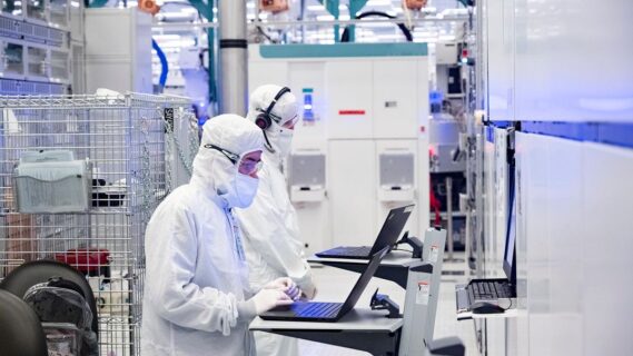
Project Fact Sheet
- Project Name: Tower Semiconductor Japan expansion, Toyama and Niigata prefectures
- Location: Uozu City, Toyama Prefecture, and Myoko City, Niigata Prefecture, Japan
- Project Value: Approximately $3 billion in Tower investment, net of about $1 billion in grants from the Government of Japan, per Tower Semiconductor’s company statement
- Client or Owner: Tower Semiconductor, operating in Japan through TPSCo
- Key Components: 300mm Silicon Photonics, Silicon Germanium and advanced packaging capacity across the repurposed Arai facility, an expanded Fab 7, and a planned new fab adjacent to Fab 7
- Procurement Model: Direct corporate investment supported by Japanese government grants, with a second facility subject to definitive agreements
- Construction Start: Track 1 conversion of the Arai facility is already underway ahead of a fourth quarter 2027 production target
- Expected Completion: Full production readiness at Arai targeted for the fourth quarter of 2027, with the new Track 2 facility expected to become accretive from 2029
- Strategic Impact: Positions Toyama and Niigata as a center of excellence for Silicon Photonics and Silicon Germanium supporting AI and data center connectivity, backed by Tower’s updated 2028 targets of $3.6 billion in revenue and $1.2 billion in net profit
Project Team
- Client or Owner: Tower Semiconductor
- Operating Subsidiary: TPSCo, the former Panasonic Semiconductor manufacturing operations
- Government Partner: Japan’s Ministry of Economy, Trade and Industry, providing approximately $1 billion in grants
- Regional Partners: Toyama Prefecture and Niigata Prefecture governments
- Main Contractor: Not yet disclosed
Frequently Asked Questions
What is Tower Semiconductor investing in its Japan expansion? Tower Semiconductor is investing approximately $3 billion, net of about $1 billion in Japanese government grants, to expand Silicon Photonics, Silicon Germanium and advanced packaging capacity in Toyama and Niigata prefectures.
Where is the Tower Semiconductor Japan expansion located? The expansion covers the Arai facility in Myoko City, Niigata Prefecture, and Fab 7 in Uozu City, Toyama Prefecture, with a planned second new facility adjacent to Fab 7.
When will the Tower Semiconductor Japan expansion be completed? Track 1, covering the converted Arai facility, is targeting full production readiness in the fourth quarter of 2027, while the larger Track 2 facility is expected to become accretive from 2029 onward.
Is the Government of Japan funding the Tower Semiconductor expansion? Yes, Japan’s Ministry of Economy, Trade and Industry is providing approximately $1 billion in grants toward the roughly $3 billion Tower Semiconductor investment.
Why is Tower Semiconductor expanding its Silicon Photonics capacity in Japan? Tower is responding to accelerating demand for optical connectivity in AI data centers, where copper interconnects can no longer keep pace with rising data rates, and the company has already signed $1.3 billion in related 2027 revenue contracts.

Leave a Reply