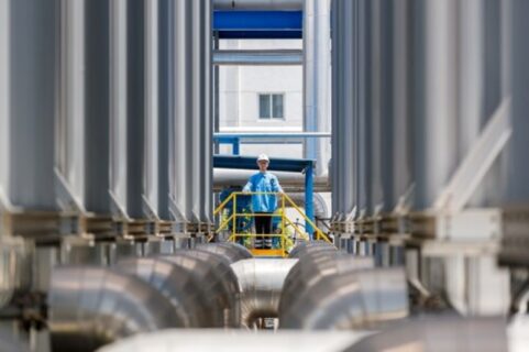
Updated June 3, 2026 – Air Liquide will build, own and operate new nitrogen gas production facilities at SK Hynix’s packaging and testing fab “P&T7” in Cheongju, Chungcheongbuk province. The facilities will start operations in late 2027, around the same time SK Hynix’s advanced packaging facility is commissioned. Air Liquide’s industrial gas production facilities will supply ultra-high-purity gases needed for manufacturing advanced memory chips, particularly high-bandwidth memory (HBM) products used in AI accelerators and data centers.
The massive Air Liquide investment complements SK Hynix’s aggressive expansion strategy which is also fast tracking the construction of a $3.8bn microchip facility in Indiana, USA. Back east, the strategy covers the accelerated development of its Yongin semiconductor cluster, adding new fabrication and advanced packaging capacity, and doubling wafer production capacity over the next five years.
SK Hynix currently leads the global HBM market with an estimated 58% share. The semiconductor company also remains a key supplier to Nvidia’s AI ecosystem, driving unprecedented demand for memory manufacturing infrastructure. The project also reinforces South Korea’s position as a global AI semiconductor hub, with industrial gas suppliers, materials manufacturers and equipment providers scaling investments alongside chipmakers to support next-gen AI memory production.
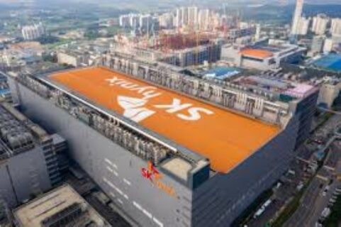
$13Bn SK Hynix P&T7 Advanced Packaging Facility in Cheongju, South Korea Begins Construction
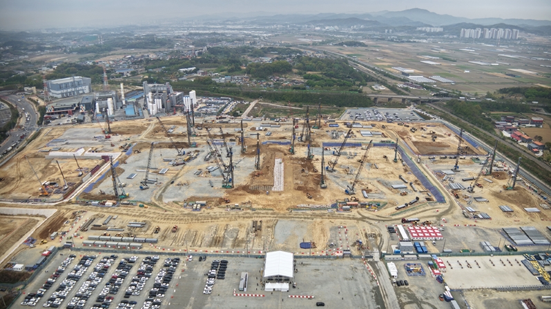
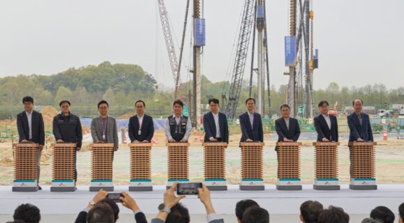
Reported April 22, 2026 – South Korean semiconductor manufacturer SK Hynix has begun construction of its new $12.9 billion ((KRW 19 trillion) “P&T7” advanced packaging facility in the city of Cheongju in South Korea. The facility is located in the Cheongju Technopolis Industrial Complex, with its development emerging as a cornerstone of SK Hynix’s strategy to scale high-bandwidth memory (HBM) production amid increasing demand driven by AI workloads. With completion scheduled for late 2027, the P&T7 plant will play an important role in resolving one of the semiconductor industry’s key challenges: advanced packaging capacity.
Project Overview
The P&T7 facility – short for Package & Test 7 – is designed as a next-generation semiconductor back-end plan. It will be responsible for transforming processed wafers into fully packaged, high-performance memory chips ready for deployment in AI systems.
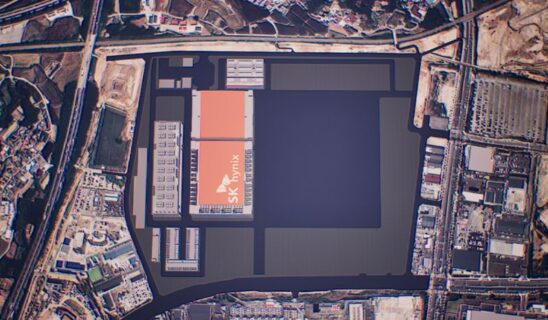
SK Hynix’s advanced packaging facility is located on a 230,000 m2 site within Cheongju Technopolis. Its development also represents one of the largest-ever investments globally in semiconductor packaging infrastructure.
Additionally, the project forms part of SK Hynix’s effort to vertically integrate its semiconductor manufacturing chain. This is through bringing front-end wafer fabrication and back-end packaging into a tightly coordinated production system.
What Will SK Hynix’s P&T7 Advanced Packaging Facility in Cheongju, South Korea Focus On
SK Hynix’s P&T7 facility in Cheongju, South Korea will specialize in advanced packaging and testing processes, including:
- High-bandwidth memory (HBM3E and next-generation HBM4) packaging
- Chip stacking and interconnect integration
- Final testing, validation, and quality assurance
- Backend processing for AI-oriented memory products
These capabilities are essential for converting raw semiconductor wafers into finished, high-performance chips used in AI servers, data centers, and advanced computing systems.
Additionally, P&T7 is expected to work in tandem with multiple existing SK Hynix plants in Cheongju, including M11, M12, M15, and the under-construction M15X fab, forming a fully integrated semiconductor production cluster.
Fact Sheet for SK Hynix P&T7 Advanced Packaging Facility in Cheongju, South Korea
Location: Cheongju Technopolis Industrial Complex in South Korea
Investment Value: $12.9 billion (KRW 19 trillion)
Developer: SK hynix
Project Type: Advanced semiconductor packaging and testing facility
Site Area: 230,000 m2
Construction Start: April 2026
Completion: Late 2027
Core Function: Advanced semiconductor packaging and testing
Key Products: HBM3E, HBM4, AI memory chips
Project Cost
Total Investment: $12.9 billion (KRW 19 trillion)
Funding: Fully financed by SK Hynix as part of its long-term capital expenditure strategy
Objective: Expand HBM production capacity
Who is Behind Construction of SK Hynix’s P&T7 Advanced Packaging Facility in Cheongju, South Korea
Developer and Owner:
- SK Hynix
Key Stakeholders:
- South Korean national government for policy and regulatory environment
- Local authorities in North Chungcheong Province
Associated Facilities:
- Existing M15 fabrication plant
- M15X next-generation DRAM/HBM fab that is under development
- Existing P&T3 packaging facility
A Look at the SK Hynix P&T7 Advanced Packaging Facility in Cheongju and South Korea’s Semiconductor Market
HBM Production and Packaging
At its core, the P&T7 project is a direct response to the increase of AI-driven computing and the resulting surge in demand for HBM. HBM, short for high-bandwidth memory, is an important component used in AI accelerators and high-performance GPUs.
Unlike traditional memory, HBM relies heavily on advanced packaging technologies such as chip stacking and through-silicon vias (TSVs). This makes packaging capacity, and not necessarily wafer production, the primary constraint in scaling output.
High-Bandwidth Memory Market
SK Hynix, already estimated to control about 60% of the global HBM market, is also moving aggressively to maintain its lead over competitors by investing in dedicated packaging infrastructure. The $12.9 billion advanced packaging hub in South Korea is testament to this.
SK Hynix P&T7 Advanced Packaging Facility Colocation with Fabrication Hubs
SK Hynix’s Cheongju P&T7 packaging facility is also linked to the adjacent M15X facility. M15X is SK Hynix’s semiconductor fabrication facility also focused on HBM. The construction of P&T7 close to M15 (and the expanded M15X) allows for easier integration between wafer processing and packaging. This proximity is also expected to improve yield rates, reduce logistics complexity, and enhance production efficiency. These are substantial advantages in a supply-constrained market.
Regional Development
Beyond corporate strategy, SK Hynix’s $13 billion semiconductor investment in South Korea also aligns with national policy of balanced regional development. More specifically, the development continues to position the city of Cheongju as a major semiconductor hub outside the Seoul metropolitan area.
Project Outlook
SK Hynix P&T7 project in South Korea will continue the transformation of Cheongju into one of the most important AI memory manufacturing hubs in the world. By integrating front-end and back-end processes within a single geographic cluster, SK Hynix is also effectively future-proofing its production model against supply chain disruptions and capacity constraints.
With the HBM market projected to grow at a compound annual rate of over 30% through 2030, the facility is also expected to come online at a very critical time. This will be alongside other builds such as the European Semiconductor Manufacturing Company’s (ESMC) fabrication plant in Dresden, poised to become one of the largest fab facilities in Europe after its completion in 2027.
Moreover, as packaging increasingly becomes the key differentiator in semiconductor performance, investments like P&T7 point toward a developing industry shift. A shift focused more on system-level integration.
Leave a Reply