Stantec has been selected to offer design and engineering services for Silicon Box’s new €3.2 billion semiconductor facility in Northern Italy.
Also in the deal is Drees & Sommer – a partner to Stantec. Together, they will come up with the architectural basis of the administration block and overall infrastructure design. This will also include the permitting services for the new state-of-the-art semiconductor assembly and test facility by Silicon Box.
Project factsheet
Client: Silicon Box
Location: Novara, Piedmont – Northern Italy
Cost: €3.2 billion
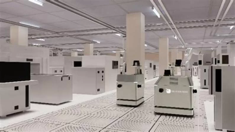
Utility: Semiconductor assembly and test facility
Designer: Stantec
Consulting and Implementation: Drees & Sommer
Architecture and Planning: CRC Hi-Tec Engineering
Start of construction date: mid-2025
Start of operations date: 2028
Semiconductor jobs created at the manufacturing facility: Approx. 1,600
Stantec named as designer for Silicon Box’s new €3.2 billion semiconductor facility in Italy
Stantec’s selection as designer for Silicon Box’s new €3.2 billion semiconductor facility in Italy was through rigorous considerations. Among these were the sustainability practices of the “global leader in sustainable design and manufacturing” – as self-acclaimed.
The lead designer also mentioned that highest environmental standards and the minimizing of environmental impact will be a priority. Europe’s Net Zero principles will also be adhered to while minimizing carbon emission and other impacts to the environment.
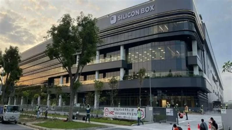
Silicon Box’s semiconductor facility in Piemont
After project unveiling in March of 2024, Silicon Box selected a site area near Novara for their new €3.2 billion semiconductor facility in June 2024. Italy was chosen because of its infrastructure, work-force, and good government and regional relations.
Poised to created about 1,600 job slots in the facility once operations begin in 2028, the facility will influence markets and innovation in the Artificial Intelligence (AI), Large Language Models (LLMs), High Performance Computing (HPC), and Electric Vehicle (EV) sectors among others. Some of these slot include engineering, technician, operator and managerial functions.
Silicon Box’s new €3.2 billion semiconductor facility in Italy will receive silicon wafers from fabrication facilities. Work in the facility will include the assembly of the wafers, packaging of complete semiconductors, and testing of the final product. These will then be shipped to companies that design chips to suit the technological needs of consumers.
Other than the 1,600 slots, more job openings will also be in the construction phase of the facility and when suppliers will be sought.
The construction phase is awaiting approval from the European Commission, after it approves of the planned government funding.
The bigger picture
Silicon Box’s new €3.2 billion semiconductor facility in Italy will not only serve the tech industry as the investment dug into pockets far too deep than one industrial sector.
It will also “align with the Italian government and the European Commission and Union’s goal […]”. A goal indicated to making the region a power-house influencing the global semiconductor market, and innovation.
The facility will play an integral part in the reclamation of the region’s 20% global semiconductor supply capacity by 2030.
Leave a Reply