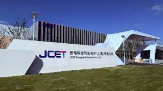
Chinese semiconductor packaging giant JCET Group has announced plans to build a new CNY7.8 billion (US$1.1 billion) advanced semiconductor chip packaging and testing plant in Lingang Special Area, Shanghai. The facility will expand the company’s high-end packaging capacity for AI computing chips, high-performance processors and next-generation semiconductor applications.
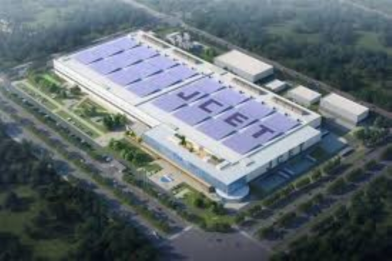
JCET chip packaging and testing plant in Shanghai: Project overview
According to company disclosures, JCET will establish a controlled subsidiary with registered capital of about CNY4 billion to develop the new facility. The plant will focus on advanced packaging and testing technologies that are increasingly important for AI accelerators. The new JCET chip plant in China will also focus on meeting data-center processors and high-performance computing applications demands.
The investment also comes as advanced packaging emerges as one of the most strategically important segments of the semiconductor value chain. As AI models become larger and more computationally demanding, chipmakers are increasingly relying on advanced packaging technologies to connect multiple chiplets and memory components into highly efficient computing systems.
JCET Shanghai Lingang Advanced Packaging and Testing Plant Factsheet
Developer: JCET Group
Location: Lingang Special Area
Investment Value: CNY7.8 billion (US$1.1 billion)
Primary Focus: AI chips, high-performance computing, advanced packaging technologies
Implementation: Multi-phase development
First Phase Completion: Second half of 2028
Key Technologies: 2.5D packaging, 3D packaging, chiplet integration, co-packaged optics, AI semiconductor packaging
China’s growing AI ecosystem and semiconductor industry
China’s semiconductor industry has been increasingly betting on investments in packaging and testing capabilities. This is as export controls and equipment restrictions continue to complicate access to the most advanced fabrication technologies. Unlike leading-edge wafer manufacturing, advanced packaging offers Chinese companies an opportunity to strengthen competitiveness through innovation in chip integration and system-level performance.
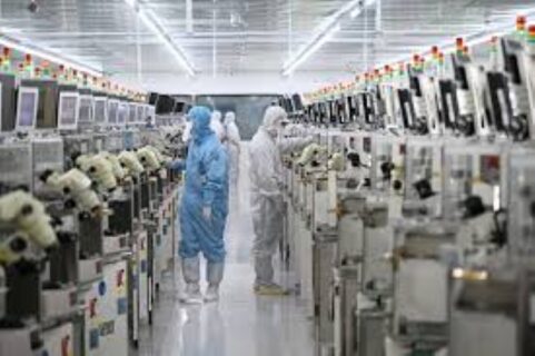
JCET is already the largest outsourced semiconductor assembly and test (OSAT) company in mainland China. The company also ranks third among the world’s leading packaging and testing providers. JCET has also been actively expanding its advanced packaging portfolio, including 2.5D and 3D packaging technologies. It has also looked into system-in-package solutions and co-packaged optics (CPO) capabilities designed for AI and high-performance computing workloads.
Additionally, the latest JCET investment in a chip packaging and testing plant in Shanghai follows recent opening of an advanced manufacturing facility in Jiangyin. The Jiangyin chip making plant is aimed at supporting AI computing, power modules and next-generation data-center applications.
JCET chip packaging and testing plant in Shanghai: Construction schedule
The Shanghai Lingang chip packaging and testing plant project by JCET will be implemented in phases. The first phase, covering factory construction and major equipment installation, is expected to be completed during the second half of 2028.
Upon completion, the facility will significantly expand JCET’s advanced packaging capacity and support the growing domestic demand for high-performance semiconductor products.
Market drivers behind JCET’s latest semiconductor investment
The investment reflects a broader industry trend as semiconductor manufacturers and packaging providers worldwide race to increase advanced packaging capacity. This demand is being fueled by:
- AI training and inference processors
- High-bandwidth memory (HBM) integration
- Advanced data-center infrastructure
- Automotive semiconductor applications
- Robotics and edge AI systems
- Co-packaged optics for next-generation networking solutions
These applications require increasingly complex packaging architectures that enable higher performance. This is while reducing power consumption and improving chip-to-chip communication speeds.
Outlook on the new JCET chip packaging and testing facility in China’s Lingang Special Area
JCET’s latest investment is the face of growing recognition that advanced packaging has become an important piece in the AI semiconductor supply chain. Furthermore, while companies such as TSMC, ASE Technology Holding and Amkor Technology continue expanding packaging capacity globally, Chinese firms are pursuing these investments in a bid to secure domestic capabilities for AI-driven semiconductor demand.
As AI data center construction continues to increase at an extraordinary rate worldwide, projects such as the Shanghai Lingang advanced chip packaging and testing plant project by JCET are expected to play a crucial role. They will support the next generation of AI chips and high-performance computing platforms. Parallel to the contribution made by semiconductor plants, China is also looking toward entire high-tech ecosystems with projects such as the 10 mega industrial parks in Guangdong. The parks will focus on AI, chips and robotics among other sectors.
Leave a Reply