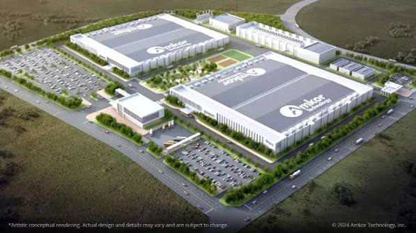
Amkor Technology is planning a second phase for its advanced semiconductor packaging and test campus in Arizona, which will provide about 60,000 square meters of cleanroom capacity and bring the total planned investment in the project to about $12 billion.
Amkor announced the second phase of its Arizona campus on September 8, 2026, following strong customer commitments that have exceeded the 33,000 square meters of cleanroom capacity initially planned for Phase 1. The company is currently planning Phase 2, which will expand the campus to approximately 93,000 square meters of cleanroom capacity once completed.
Amkor is developing the campus in multiple phases to meet growing U.S. demand for advanced semiconductor packaging and test services. The Arizona campus will include wafer bumping, probing, assembly and testing capabilities, creating a domestic manufacturing platform for advanced semiconductor devices.
Phase 2 construction planned for 2027
Construction of Phase 2 of the campus is expected to start late in 2027, with completion scheduled for the end of 2029.
The expansion will boost manufacturing capability of the campus and provide employment opportunities for over 3,500 Arizona-based employees for Phase 1 and Phase 2. The company noted that the 170 acre campus has been built to enable additional expansion of capacity based on customer requirements.
Amkor president and CEO Kevin Engel said that the next phase shows customer confidence in Amkor and increasing significance of advanced packaging for semiconductor manufacturing.
The campus will create a turnkey domestic manufacturing platform for customers with a combination of several stages of advanced packaging and testing services in the U.S.
Arizona campus strengthens U.S. domestic semiconductor manufacturing
Amkor’s Arizona campus project is part of its plan for building the first advanced semiconductor outsourced assembly and test production facility in the U.S.
Development of the campus is also a step towards building more domestic manufacturing facilities for semiconductors. The company has stated that its Arizona campus is complementary to front-end wafer fabrication in the state, which creates an opportunity to link wafer fabrication with advanced packaging and testing within the U.S. semiconductor manufacturing value chain.
In June 2026, Amkor and TSMC entered into a 10-year deal to enhance advanced semiconductor packaging capabilities in Arizona. As per the agreement, TSMC will be purchasing advanced packaging and testing services from Amkor for addressing increasing demands for advanced semiconductor devices used in high-performance computing, artificial intelligence, and advanced electronics.
In May 2026, Amkor expanded the physical area of its campus development project with an acquisition of 67 additional acres of land adjoining its existing 104-acre campus, resulting in a total of about 171 acres of land. Additional land has been acquired for future expansions.
Construction of the first manufacturing facility is underway
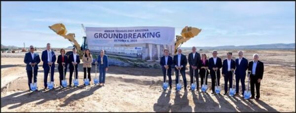
Construction of the first manufacturing facility is underway. Amkor has stated that construction of foundation is advancing towards steel construction and Phase 1 is still on target for completion in 2027.
The enlarged campus will be able to provide advanced packaging and testing services for artificial intelligence, high-performance computing, automotive and communications applications. Amkor’s investment program in 2026 also includes substantial spending on capital expenditures for its Arizona campus with the company estimating about $2.5 billion to $3 billion for 2026.
With Phase 2 added in Arizona, Amkor will build a much larger U.S. advanced semiconductor manufacturing campus, expanding domestic cleanroom capacity to meet growing demand for chip packaging.
Additionally, the semiconductor manufacturing buildout is also gaining momentum beyond the United States. In the Netherlands, ASML has broken ground on its new BIC North industrial campus in Eindhoven, launching a multi-phase development that could eventually span approximately 350,000 square meters and accommodate up to 20,000 workplaces.
Project factsheet: Amkor Arizona Advanced Packaging and Test Campus
- Location: Arizona, United States
- Developer: Amkor Technology, Inc.
- Total planned investment: Approximately $12 billion
- Phase 1 cleanroom capacity: Approximately 33,000 square meters
- Phase 2 additional cleanroom capacity: Approximately 60,000 square meters
- Total planned cleanroom capacity: Approximately 93,000 square meters
- Campus size: Approximately 170 acres
- Phase 2 construction start: Expected late 2027
- Phase 2 completion: Expected by the end of 2029
- Expected workforce: More than 3,500 Arizona-based employees across Phases 1 and 2
- Capabilities: Wafer bump, probe, advanced packaging, assembly and test
- Construction status: Phase 1 under construction; Phase 2 planned



Leave a Reply