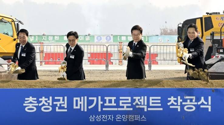
Samsung has started construction on a 6 trillion won ($4.1 billion) Asan chip packaging plant. The plant is located at Samsung’s Onyang campus in Asan, South Chungcheong Province. President Lee Jae-myung and Samsung Executive Chairman Jay Y. Lee joined in the groundbreaking ceremony for the Chungcheong mega-project on Nov. 12. The ceremony includes a three-part build. The semiconductor packaging plant and an advanced display line follow in Asan, and a substrate facility follows in Sejong.
The Onyang plant is estimated to cost 6 trillion won, or $4.1 billion. In addition, Samsung is investing a total of 40 trillion won, or about $27.5 billion, in advanced equipment investments in stages. Industry Minister Kim Jung-kwan and Asan Mayor Oh Se-hyun attended the ceremony with the Asan substrate partner, Daeduck Electronics.
Other Projects
Other than industrial, South Korea is also advancing the needed energy projects to facilitate operations on these projects such as plans to expand its nuclear power generation capacity through the development of two additional large-scale reactors, as part of its long-term strategy to address rising electricity demand and energy security objectives. The proposal forms part of the country’s broader national power supply roadmap, which aims to balance industrial growth, decarbonization commitments, and grid reliability. The reactors are expected to support stable baseload generation while complementing renewable energy expansion and emerging hydrogen production initiatives.
Scope of the Samsung Asan chip packaging plant
The technical ambition for the site was set by Executive Chairman Jay Y. Lee. The campus will become a hub for cutting-edge high-bandwidth memory, the “heart” of AI semiconductors, he said. The flagship product of the plant is TSP (Test & System Package) that anchors those pushes. Meanwhile, the chairman signed a display of it at the ceremony.
President Lee said that corporate investment should be converted into job creation and economic revitalization in the local community. We will focus our policy capacities on the completion of the mega-project as a true balanced national development. Furthermore, the president promised that the central and local governments would work as a single team until the end regarding permits, licenses and basic infrastructure like power and water.
In the meantime, the chairman broadened the scope beyond Chungcheong. Jay Y. Lee said that the Chungcheong region is not the only place where they will be looking for mega-projects, but also in the Honam and Yeongnam regions. The source does not mention a completion date or hiring target for the Onyang plant, however, so this story does not include them.
Outlook for the Chungcheong mega-project
The groundbreaking marks the first time the mega-project has been announced, planned and built simultaneously at three locations. Consequently, Asan receives the packaging plant and display line, while Sejong is ready to build the AI-server substrate plant. The 40 trillion won equipment cost is phased in on top of the $4 billion building. The government, therefore, has to provide the power and water facilities that Samsung’s fabs will require. In addition, Samsung has to adhere to its phased equipment schedule.
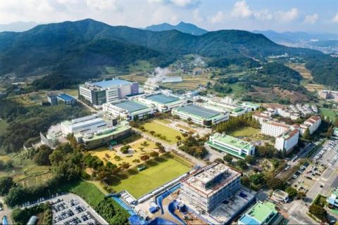
Project Overview: Samsung Asan chip packaging plant
- Plant Value: 6 trillion won ($4.1 billion)
- Location: Onyang campus, Asan, South Chungcheong
- Developer: Samsung Electronics
- Programme: Chungcheong mega-project
- Equipment Investment: 40 trillion won ($27.5 billion)
Scope
- Advanced packaging plant at Onyang
- Advanced display production line, Asan
- AI-server substrate facility, Sejong
- Phased equipment install to follow
Project Highlights
- Targets high-bandwidth memory hub
- Flagship product: TSP packaging
- Balanced national development push
- Government backs permits, power, water
Key Developments
- Groundbreaking held Nov. 12
- President Lee attended ceremony
- Jay Y. Lee pledged regional expansion
- Daeduck Electronics joined the build
Key Challenges
- Equipment spending spans phases
- Power and water infrastructure needed
- Sejong facility still to rise
- No completion date disclosed
Outlook
- Three sites build in parallel
- Equipment phases follow construction
- Honam and Yeongnam eyed next
- HBM capacity anchors AI push

Leave a Reply