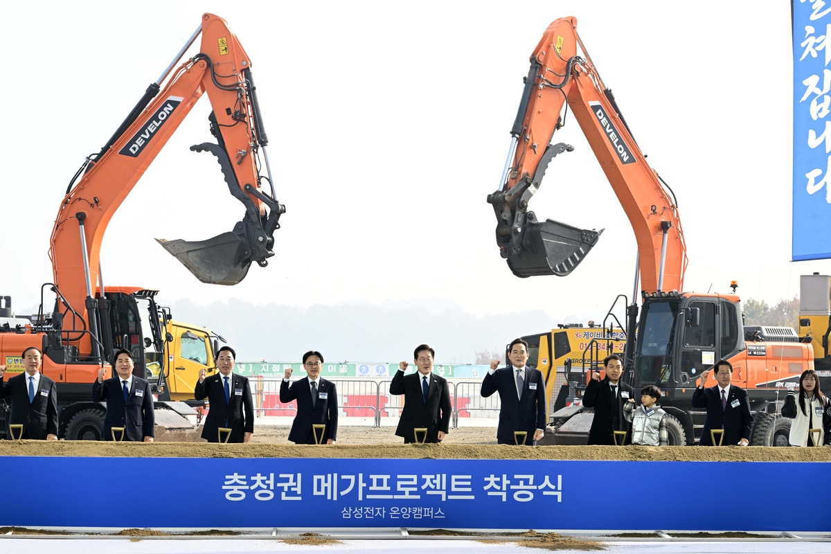
Samsung Electronics broke ground on November 12, 2026, on a 6 trillion won ($4.48 billion) high-bandwidth memory chip packaging plant at its Onyang campus in Asan, South Korea. The company has accelerated target operations to June 2028, one year ahead of its initial schedule, to relieve global bottlenecks in artificial intelligence server memory.
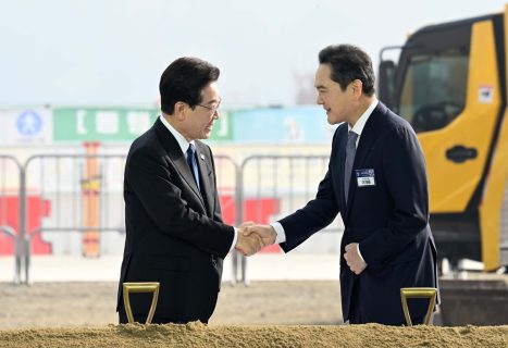
Speaking at the ceremony in South Chungcheong Province, President Lee Jae Myung said the construction outlay will be followed by roughly 40 trillion won ($30 billion) in advanced equipment purchases. The facility anchors Samsung Electronics‘ broader 60 trillion won regional semiconductor program, which forms part of the $90 billion Chungcheong industrial construction roadmap unveiled by Samsung Group affiliates in July 2026.
Three-Story Cleanroom Scale and Production Scope
Plans presented at the groundbreaking outline three floors of cleanroom space covering about 31,000 square meters, an area equivalent to more than four standard football pitches. Inside the complex, Samsung Electronics will install five back-end production lines and expand total campus packaging floor area to 420,000 square meters.
Back-end packaging forms the final manufacturing stage where individual semiconductor dies are stacked, bonded, and tested before shipment. High-bandwidth memory modules built at Onyang, including next-generation HBM4E chips, stack multiple DRAM layers vertically to boost data transfer speeds and cut power consumption in hyperscale servers.
Why Did Samsung Move Startup Forward to 2028?
Surging global demand for AI computing hardware has tightened advanced packaging capacity across South Korea and Taiwan. Pulling target operations forward to June 2028 mirrors parallel schedule accelerations across Samsung’s Yongin semiconductor cluster as the chipmaker races rivals to secure hyperscaler supply contracts.
Korean financial outlet MoneyToday reported sequential facility outlays of 4.6 trillion won to 6 trillion won for the initial building works before the 40 trillion won ($30 billion) equipment rollout. During a public-private megaproject review meeting held at the Onyang site after the ceremony, President Lee Jae Myung said, “What matters now is action, not words. Implementation, not promises.”
Regional Supply Chain and Supplier Investment
Groundbreaking at Onyang marks the first physical construction milestone in a wider 144 trillion won ($108.4 billion) investment drive by four Samsung affiliates across central South Korea. Fellow subsidiaries Samsung Display, Samsung SDI, and Samsung Electro-Mechanics are simultaneously advancing display, next-generation battery, and substrate projects in Asan, Cheonan, and Sejong.
According to Samsung Electronics projections reported by Maeil Business Newspaper, the company’s 60 trillion won Chungcheong expansion will generate an estimated 17.3 trillion won in economic output and create 11,000 new jobs across operations and partner firms. President Lee added that 112 supplier companies in semiconductors and biotechnology plan to invest an extra 23.6 trillion won in the region.
Elsewhere across Samsung Group’s industrial engineering arm, affiliate Samsung E&A is executing the $1.7 billion TA’ZIZ methanol plant contract in Al Ruwais, where project sponsors closed $2 billion in financing in May 2026 ahead of targeted 2028 completion.
Project Overview
-
Project Name: Samsung Electronics Onyang HBM Packaging Plant
-
Developer: Samsung Electronics
-
Location: Onyang Campus, Asan, South Chungcheong Province, South Korea
-
Project Type: Semiconductor Back-End Packaging Facility (High-Bandwidth Memory)
-
Project Value: 6 trillion won ($4.48 billion) initial construction; 40 trillion won ($30 billion) planned equipment investment
-
Cleanroom Area: Approximately 31,000 square meters across three floors
-
Total Floor Area: 420,000 square meters (expanded campus packaging footprint)
-
Production Lines: Five packaging lines (including HBM4E)
-
Status: Under construction (groundbreaking held November 12, 2026)
-
Target Completion: June 2028 (accelerated by one year)
-
Regional Program Jobs: 11,000 projected jobs across Samsung Electronics and suppliers
-
General Contractor: Not publicly disclosed
Project Team
-
Developer and Operator: Samsung Electronics
-
Parent Conglomerate: Samsung Group
-
Display Affiliate (Regional Program): Samsung Display
-
Battery Affiliate (Regional Program): Samsung SDI
-
Components Affiliate (Regional Program): Samsung Electro-Mechanics
-
Government Partner: Government of the Republic of Korea
-
General Contractor: Not yet disclosed


Leave a Reply