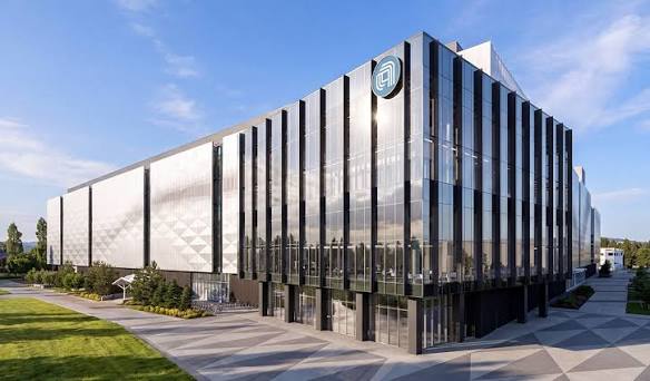
Applied Materials has unveiled a $5 billion research complex in Silicon Valley where some of the world’s fiercest semiconductor rivals will work side by side to develop the technologies behind tomorrow’s AI chips.
The Equipment and Process Innovation and Commercialization Center, or EPIC, opened at Applied’s Sunnyvale campus on Monday, October 12, 2026. The company describes it as the world’s largest facility dedicated to collaborative semiconductor process technology and manufacturing-equipment research and development.
The facility brings together chipmakers TSMC, Intel, Samsung Electronics, Micron and SK hynix as founding partners. They are joined by Broadcom, Advantest, SCREEN, KIOXIA and Besi, along with researchers from Arizona State University, Rensselaer Polytechnic Institute, Stanford University, UC Berkeley and UCLA.
For an industry usually defined by secrecy, patents and intense competition, EPIC represents an unusual experiment: rival companies sharing a research ecosystem while retaining control over their own projects and intellectual property.
Why AI needs a bigger lab
The immediate driver is artificial intelligence. Training and running large AI models requires enormous computing power, high-bandwidth memory and energy-efficient data movement between processors, memory chips and networking systems.
That demand is pushing chipmakers beyond the familiar race to shrink transistors. Future performance gains increasingly depend on new materials, low-resistance wiring, advanced memory, 3D chip stacking and advanced packaging—technologies that must work together at atomic scale.
Applied Materials chief executive Gary Dickerson said the demands of high-performance computing were creating “unprecedented complexity” across the chipmaking roadmap. The company argues that no single firm can solve those challenges alone.
EPIC is designed to remove a long-standing bottleneck in semiconductor development. Traditionally, materials research, equipment development, process integration and pilot production happen in separate organisations or facilities, with time-consuming handoffs between each stage. Applied wants scientists, engineers, equipment makers and customers to develop and test technologies in the same place.
A $5bn bet on collaboration
The Sunnyvale building covers 600,000 square feet and contains nearly four acres of cleanroom space. Applied says its construction required more than six million work hours, underlining the scale of the engineering challenge involved in building a facility where experimental chip processes can be tested close to manufacturing conditions.
The $5 billion figure should be read carefully. Applied describes EPIC as a $5 billion capital investment, but says spending is expected to scale to approximately that level as customer projects begin. In other words, it is a projected total investment rather than a confirmed amount already spent.
The project also took longer than originally planned. Applied first announced EPIC in May 2023, when it said it expected to invest up to $4 billion over seven years and complete the facility by early 2026. The company later raised the expected investment to about $5 billion as more partners and projects joined.
At the time of the original announcement, Applied said the project could create up to 2,000 engineering jobs in Silicon Valley and support thousands more across the wider semiconductor supply chain. Those figures remain projections rather than confirmed employment outcomes.
Rivals under one roof
The most striking feature of EPIC is its partner list. TSMC and Intel compete directly in advanced chip manufacturing, while Samsung, Micron and SK hynix compete in memory. Yet all five are founding partners in the same research center.
TSMC chairman and chief executive C.C. Wei said the partnership would give the company early access to equipment technologies needed beyond today’s 2-nanometer generation, including low-resistance wiring and advanced packaging.
Intel chief executive Lip-Bu Tan said the company sees a route to more than one trillion transistors in a package by 2030, but added that rising research costs and growing architectural complexity require closer work with equipment suppliers.
Memory makers have a similarly direct interest. Micron and SK hynix have announced partnerships with Applied focused on next-generation DRAM, high-bandwidth memory and NAND storage—technologies central to AI data centers.
Samsung’s participation adds another major memory and logic manufacturer to the platform. The company said it sees EPIC as a way to accelerate development across leading-edge logic, memory and advanced packaging.
What happens inside
EPIC is not a conventional factory. It is intended to function as a bridge between laboratory research and high-volume manufacturing.
Partners are expected to bring their own engineers and technology roadmaps into the facility, working with Applied researchers in secure programmes. The goal is to identify problems earlier, test new materials and equipment in manufacturing-like conditions, and reduce the risk that a promising laboratory breakthrough fails when it reaches a commercial fab.
Applied says this model should benefit both sides. Chipmakers gain earlier access to emerging materials and equipment, while Applied gains visibility into the technical problems its customers will face over several product generations.
The company has also positioned EPIC as part of a wider effort to strengthen U.S. semiconductor research. When it announced the project in 2023, Applied said EPIC was expected to connect with a planned U.S. National Semiconductor Technology Center, though the latest announcement focuses mainly on the facility’s commercial partnerships.
The test ahead
The opening is a major milestone, but the real test is whether EPIC can deliver what it promises: faster movement from research breakthrough to volume production.
Semiconductor development is expensive, slow and highly uncertain. New materials can behave differently at nanometre scale, and even promising technologies can fail to achieve the yields required for mass production. EPIC’s value will depend on whether shared experimentation genuinely reduces those failures.
For now, the center gives Applied a powerful position at the center of the AI-chip supply chain. It also signals that the next phase of the AI race will not be won only by designing faster processors, but by reinventing how the industry invents, tests and manufactures the technologies beneath them.
If EPIC works, the world’s biggest chipmakers may have found a way to cooperate just enough to compete more effectively against the physical limits of computing. If it does not, it will still stand as one of the clearest signs that AI has made semiconductor innovation too complex—and too expensive—for any company to pursue alone.
U.S. semiconductor construction boom
Additionally, the Applied Materials’ new EPIC Center adds a research-and-development counterpart to the U.S. semiconductor construction boom now taking shape around the country. While EPIC will bring chipmakers, equipment suppliers and universities together in Silicon Valley to develop next-generation AI-chip technologies, SK hynix is already building a more than $4 billion advanced memory-packaging facility in West Lafayette, Indiana, where it broke ground in August. The two projects reflect different stages of the same AI supply chain: EPIC is designed to accelerate the invention and commercialization of new chipmaking processes, while SK hynix’s Indiana plant is intended to turn advanced high-bandwidth memory into U.S.-based production capacity for AI data centers.
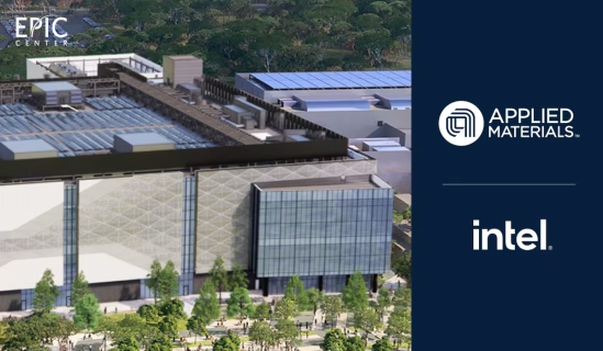
Applied Materials EPIC Center: Quick Facts
- Applied Materials unveiled its EPIC Center in Sunnyvale, California, on October 12, 2026.
- EPIC stands for Equipment and Process Innovation and Commercialization Center.
- It is described as the world’s largest facility for collaborative semiconductor process and equipment R&D.
- Total investment is expected to reach about $5 billion as customer projects begin.
- The 600,000-square-foot facility includes nearly four acres of cleanroom space.
- It aims to speed up development of AI chips, advanced memory, packaging and next-generation manufacturing technologies.
Key partners
- Founding chipmakers: TSMC, Intel, Samsung Electronics, Micron and SK hynix.
- Innovation partners: Broadcom, Advantest, SCREEN, KIOXIA and Besi.
- Universities: Arizona State, RPI, Stanford, UC Berkeley and UCLA.
Why it matters
- AI requires faster, more energy-efficient chips and memory.
- EPIC brings rival chipmakers, equipment suppliers and researchers into one facility.
- The goal is to move breakthroughs from the lab to high-volume manufacturing faster.
- The project was first announced in May 2023 with a planned investment of up to $4 billion.

Leave a Reply